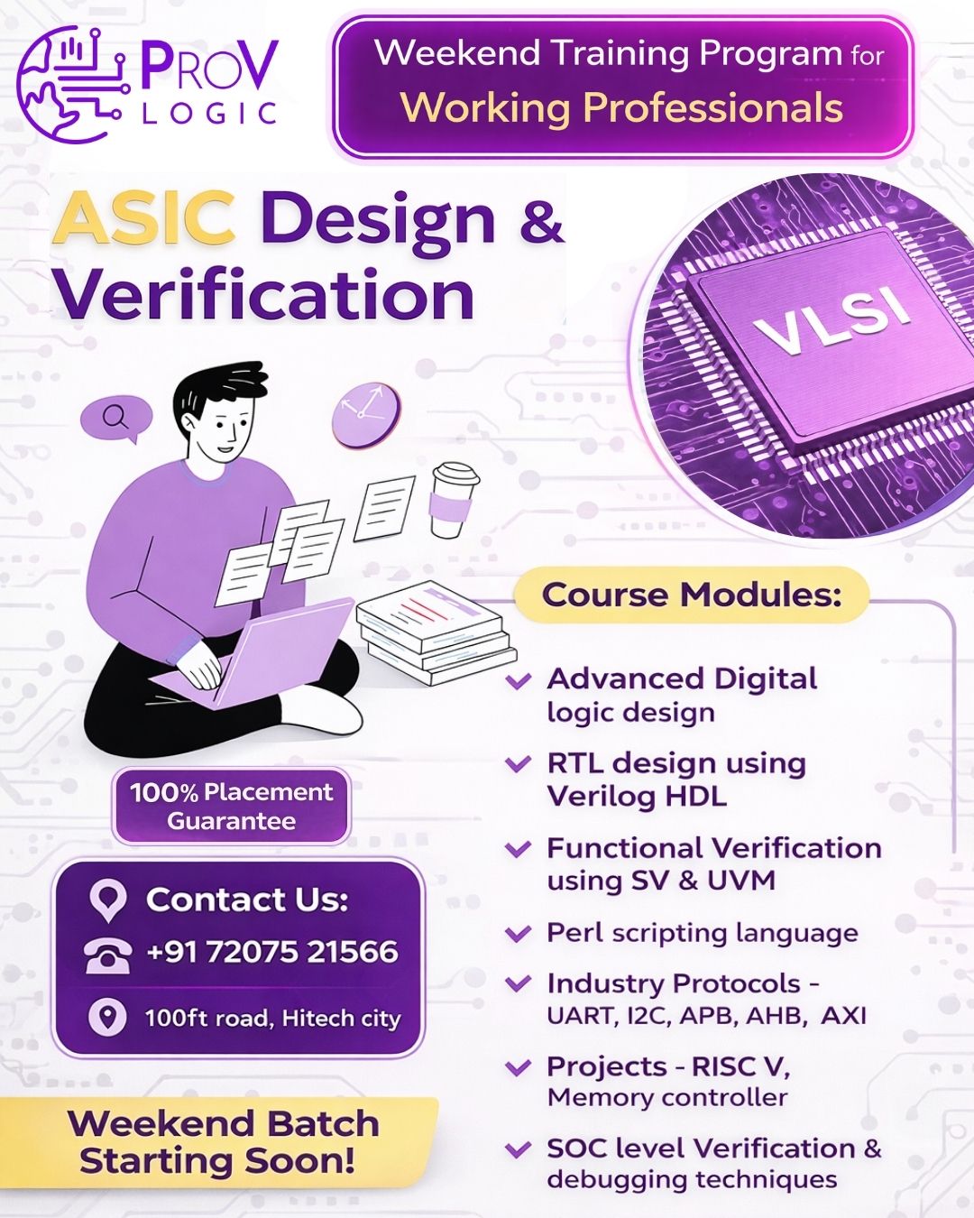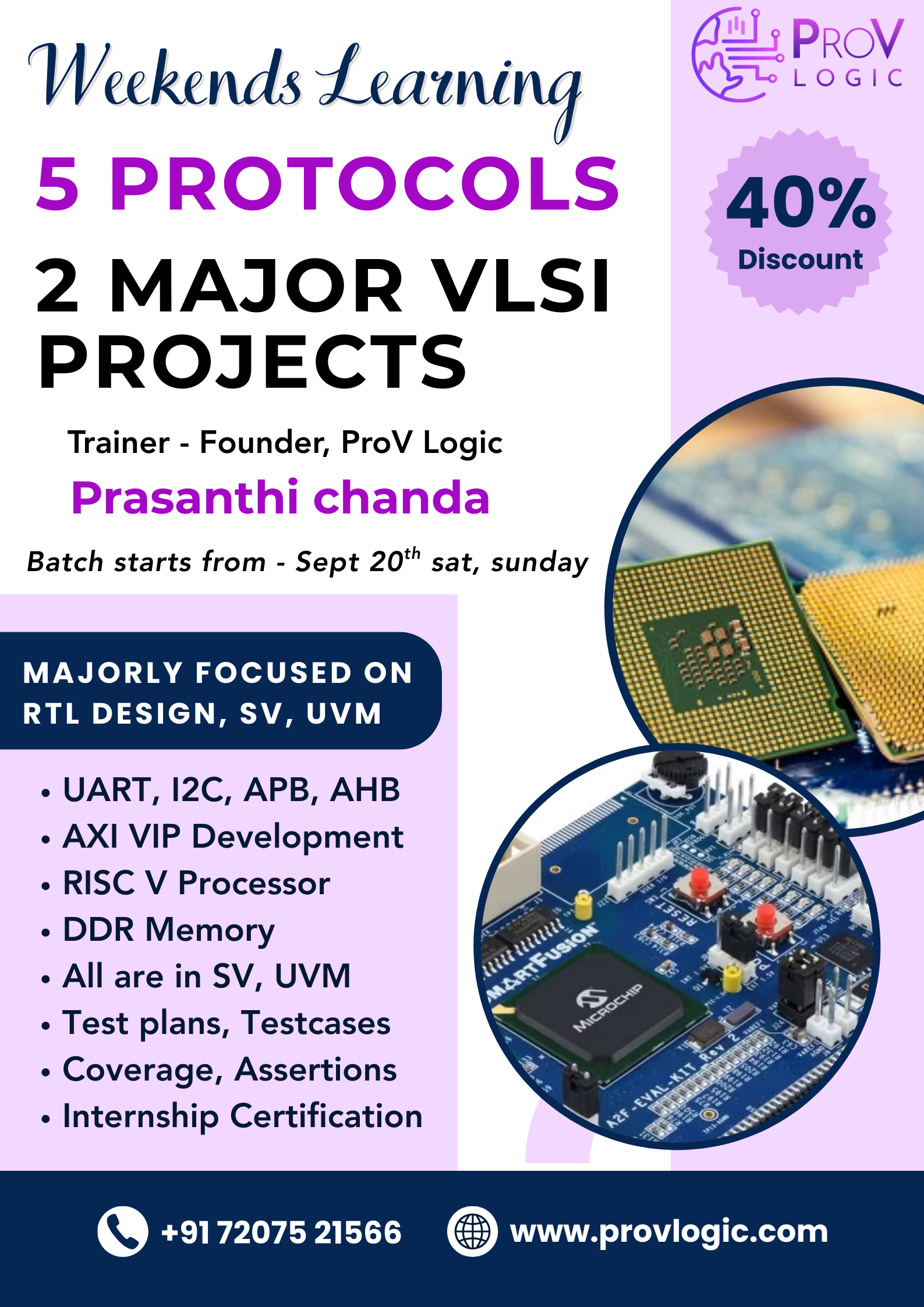
We don't just teach VLSI - we train you with real-time applications and hands-on tools used in the industry. Every concept is explained through practical implementation to make you job-ready from Day 1.


WE TRAIN • WE INNOVATE • WE DESIGN
ProV Logic is a premier VLSI training and career development institute, built with a vision to empower, educate, and elevate aspiring engineers into top-tier semiconductor professionals. We are committed to delivering high-quality, industry relevant education that equips learners with both technical expertise and real-world confidence.

Chosen by
Learners
The VLSI Career Launchpad is a 3-month, fast-track program designed for college students who want to break into the semiconductor industry with practical, project-driven training. The projects and protocol integration will help you land your first stipend-based internship.
Program Highlights:
✅ Duration: 12 Weeks (3 Months)
✅ Course Fee: 19k if qualified in the entrance test
✅ Eligibility: ECE/EEE/CSE Students (1st, 2nd, 3rd Years)
✅ Outcome: Guaranteed internship in Digital Design / RTL / Verification
Curriculum Roadmap:
Month 1 – Foundations & RTL Basics
Month 2 – SystemVerilog & Processor Design
Month 3 – Protocols & Final Integration
Deliverables & Portfolio:
🎓 By the end of the program, students will have:
1 Major Project: RISC-V CPU Implementation
1 Protocol Project: UART Design
1 Integrated Final Demo: CPU communicating via UART
GitHub Repository with HDL code + documentation
Stipend-based internship for top performers
Experience our teaching methodology and interact with our faculty. Learn about career opportunities in VLSI and get your questions answered by industry experts.
ProV Logic Institute HiTech city, Madhapur, Hyderabad, Telangana 500081

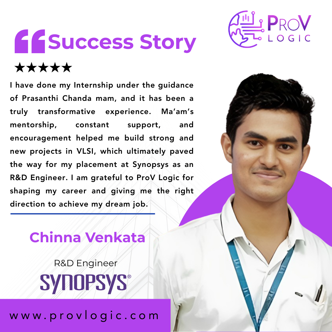


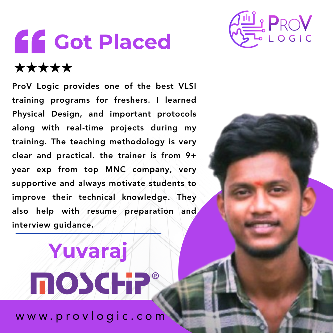


ProV Logic's VLSI course gave me the perfect foundation to start my career. The hands-on projects using industry tools were invaluable. Within 3 months of completing the course, I got placed at Intel.
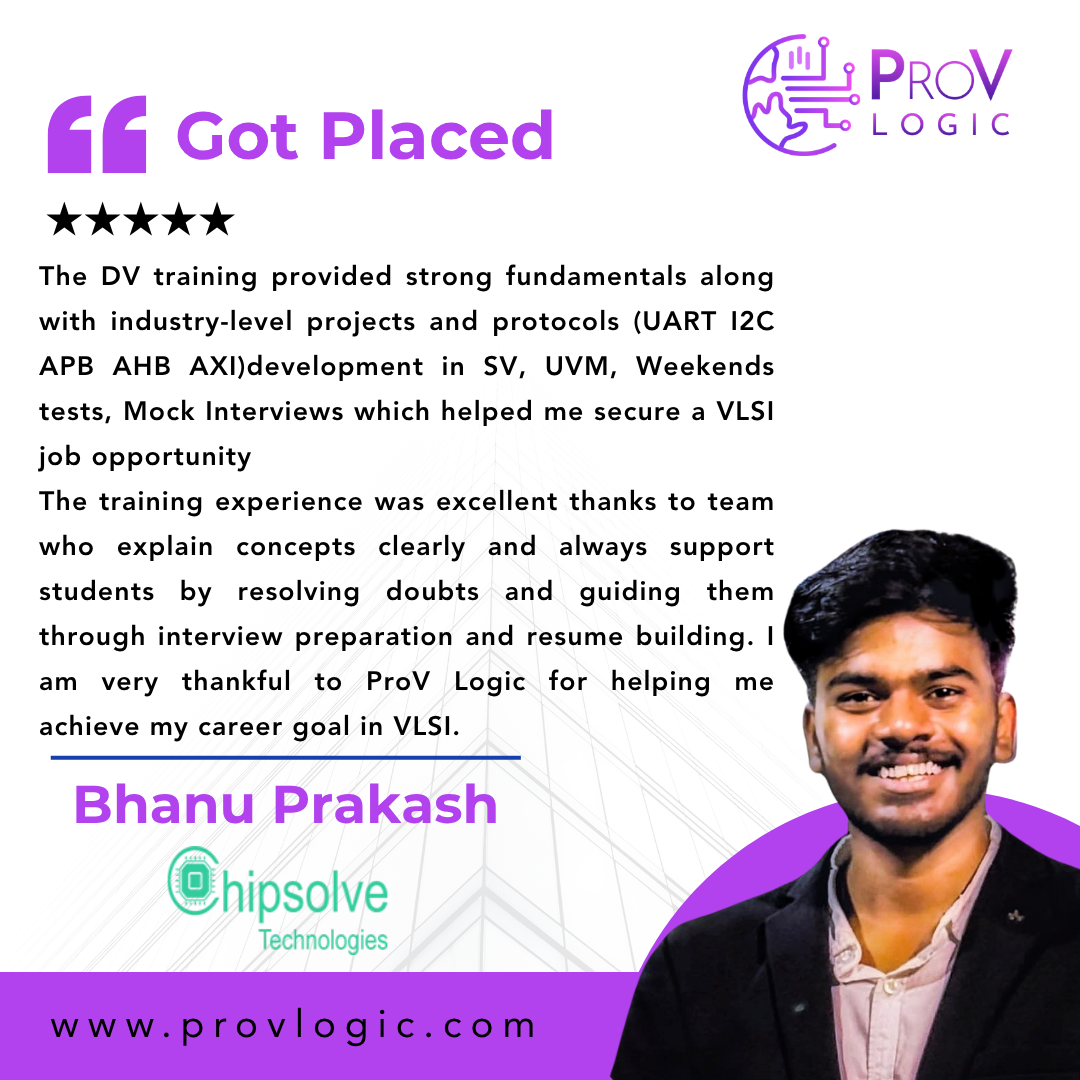
The UVM verification course transformed my career. The faculty's industry experience helped me understand real-world challenges. The interview preparation sessions were particularly helpful for cracking Nvidia's hiring process.
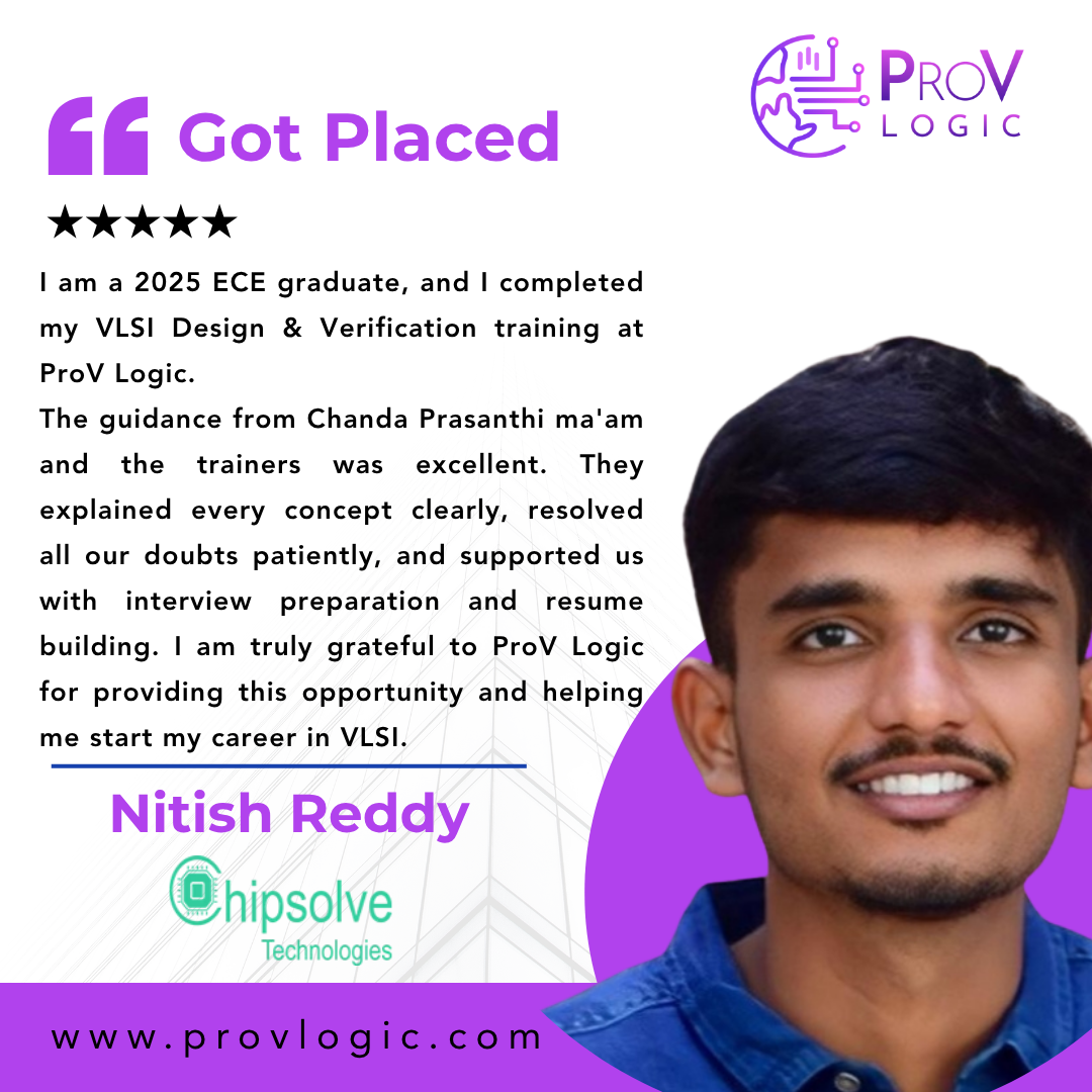
Coming from an ECE background, the Physical Design course helped me bridge the gap between academic knowledge and industry requirements. The placement cell at ProV Logic connected me with multiple opportunities.
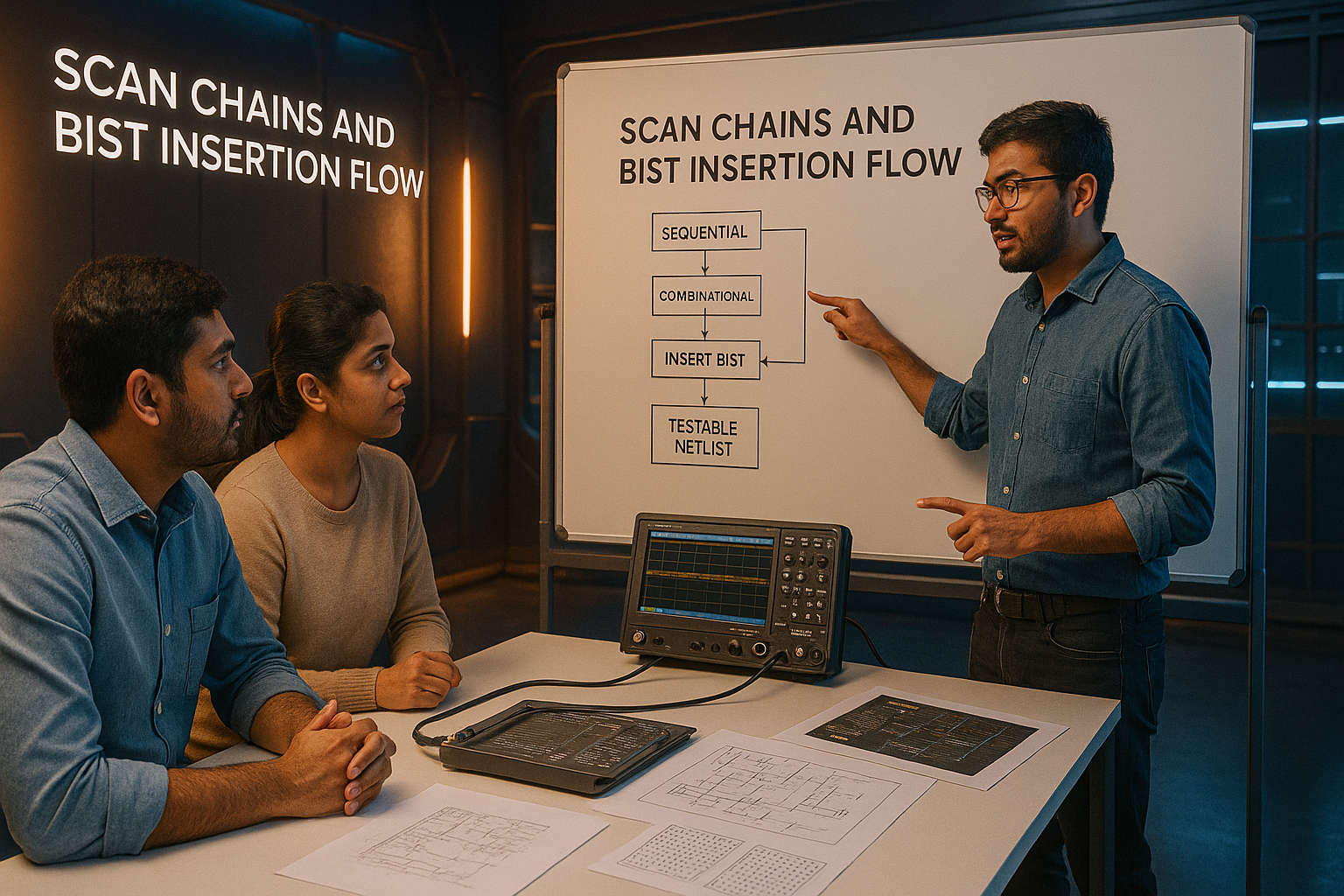
The DFT course was exceptionally well-structured with real industry projects. The mentors provided personalized guidance that helped me secure a position at Texas Instruments within 2 months of course completion.
ProV Logic's hands-on approach to RTL design gave me the confidence to tackle complex design challenges. The industry-relevant projects were exactly what recruiters were looking for.


ProV Logic Institute stands out as a premier VLSI training provider with industry-aligned curriculum, experienced faculty, and excellent placement record.
Learn from instructors with 10+ years of experience in semiconductor companies like Intel, Qualcomm, and Nvidia